| |
|
Highlights |
 |
|
Placement accuracy 5 µm*
Components from 0.125 mm x 0.125 mm to 100 mm x 100 mm*
Working area up to 450 mm x 234 mm*
Supports wafer/substrate sizes* up to 8" *
Supports bonding forces up to 400 N*
Can be configured as a hot air rework system
Manual and semi-automatic configurations
|
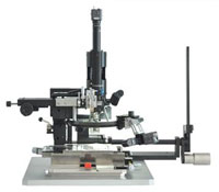
FINEPLACER® lambda
|
|
|
| |
Features |
|
|
Benefits |
|
| |
Automated processes
Overlay vision alignment system (VAS) with fixed beam splitter
Integrated Process Management (IPM)
Real time process observation camera
Advanced system software with adaptive process library
Process transfer from system to system
Process flexibility due to modular concept
|
|
|
Hands-off die placement, user independent process operation
Outstanding placement accuracy and instant operation without adjustments
Synchronized control of all process related parameters: force, temperature, time, power, process environment, light and vision
Immediate visual feedback reduces process development time
Fast and easy process development, process recording and reporting, photo capture
Process transfer from R&D to production saves time, guarantees reliable results
One system handles a wide variety of applications
|
|
| |
Technologies |
|
|
Applications |
|
| |
Thermocompression
Thermosonic
Ultrasonic
Soldering (AuSn, C4, Indium, eutectic)
Adhesive technologies
Curing (UV, thermal)
Mechanical assembly
|
|
|
Laser diode, laser bar bonding
VCSEL, photo diode assembly
LED bonding
Micro optics assembly
MEMS packaging
Sensor packaging
3D packaging
Wafer level packaging (W2W, C2W)
Chip on glass, chip on flex
Flip chip (face down)
Precise die bonding (face up)
|
|
| |
Technical SpecificationsApplications |
|
| |
Placement accuracy*: |
5 µm |
|
| |
Field of view (min)1: |
1.6 mm x 1.2 mm |
|
| |
Field of view (max)1: |
20 mm x 15 mm |
|
| |
Component size (min): |
0.125 mm x 0.125 mm |
|
| |
Component size (max): |
40 mm x 40 mm |
|
| |
Theta fine travel: |
± 6° |
|
| |
Z-travel |
10 mm |
|
| |
Working area1: |
280 mm x 117 mm |
|
| |
Heating temperature (max)1,2*: |
400 °C |
|
| |
Bonding force (max)1,2*: |
400 N |
|
| |
|
|
|


