| |
|
Highlights |
 |
|
Sub-micron placement accuracy
Unique optical resolution
Handles ultra small components
Special tools allow object sizes down to 5 µm*
Supported substrate size up to 6" *
Closed loop force control*
Small footprint and compact design
Optics movement with programmable positions
|
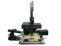
FINEPLACER® lambda
|
|
|
| |
Features |
|
|
Benefits |
|
| |
Automated processes
Overlay vision alignment system (VAS) with fixed beam splitter
Robust construction and modular design
Integrated Process Management (IPM)
Real time process observation camera
Adaptive process library
Process transfer from system to system
Virtually unlimited range of advanced bonding technologies
|
|
|
Hands-off die placement, user independent process operation
Outstanding placement accuracy and instant operation without adjustments
Provides high level of reproducibility and application flexibility
Synchronized control of all process related parameters: force, temperature, time, flow, power, process environment, light and vision
Immediate visual feedback reduces process development time
Fast and easy process development
Process transfer from R&D to production saves time, guarantees reliable results
ROI savings - one machine for all applications
|
|
| |
Technologies |
|
|
Applications |
|
| |
Thermocompression
Thermosonic
Ultrasonic
Soldering (AuSn, C4, Indium, eutectic)
Adhesive technologies
Curing (UV, thermal)
Mechanical assembly
|
|
|
Laser diode, laser bar bonding
VCSEL, photo diode assembly
LED bonding
Micro optics assembly
MEMS packaging
Sensor packaging
3D packaging
Wafer level packaging (W2W, C2W)
Chip on glass, chip on flex
Flip chip (face down)
Precise die bonding (face up)
|
|
| |
Technical SpecificationsApplications |
|
| |
Placement accuracy*: |
± 0.5 µm |
|
| |
Field of view (min)1: |
0.4 mm x 0.3 mm |
|
| |
Field of view (max)1: |
6 mm x 4.5 mm |
|
| |
Component size (min): |
0.1 mm x 0.1 mm |
|
| |
Component size (max): |
15 mm x 15 mm |
|
| |
Theta fine travel: |
± 5° |
|
| |
Z-travel |
10 mm |
|
| |
Working area1: |
190 mm x 52 mm |
|
| |
Bonding force range2*: |
0.1 N - 400 N |
|
| |
Heating temperature (max)1,2*: |
400 °C |
|
| |
|
|
|


