| |
|
Highlights |
 |
|
Sub-micron placement accuracy*
Handles ultra small to very large components
Fully-automated operation and assembly process
Supports wafer/substrate sizes up to 12" *
Supports bonding forces up to 500 N*
Highly flexible platform architecture
Small footprint and compact design
Long-term stability
|
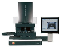
FINEPLACER® femto
|
|
|
| |
Features |
|
|
Benefits |
|
| |
Automated pattern recognition, alignment and bonding
Overlay vision alignment system with fixed beam splitter in combination with automatic field extension and zoom
Integrated Process Management (IPM)
Adaptive process library
Live process observation camera
Virtually unlimited range of advanced bonding technologies
|
|
|
Fully automated, user independent process
Outstanding placement accuracy and instant operation without adjustments
Synchronized control of all process related parameters: force, temperature, time, power, process environment, light and vision
Fast and easy process development
Immediate visual feedback reduces process development time
ROI savings - one machine for all applications
|
|
| |
Technologies |
|
|
Applications |
|
| |
Thermocompression
Thermosonic
Ultrasonic
Soldering (AuSn, C4, Indium, eutectic)
Adhesive technologies
Curing (UV, thermal)
Mechanical assembly
|
|
|
Laser diode, laser bar bonding
VCSEL, photo diode assembly
LED bonding
Micro optics assembly
MEMS packaging
Sensor packaging
3D packaging
Wafer level packaging (W2W, C2W)
Chip on glass, chip on flex
Flip chip (face down)
Precise die bonding (face up)
|
|
| |
Technical SpecificationsApplications |
|
| |
Placement accuracy*: |
± 0.5 µm |
|
| |
Field of view (min)1: |
0.27 mm x 0.2 mm |
|
| |
Field of view (max)1: |
3.2 mm x 2.4 mm |
|
| |
Component size (min): |
0.1 mm x 0.1 mm |
|
| |
Component size (max): |
100 mm x 100 mm |
|
| |
Theta fine travel: |
± 9° / 3.5 µrad |
|
| |
Z-travel / resolution: |
10 mm / 0.2 µm |
|
| |
Y-travel / resolution: |
150 mm / 0.1 µm |
|
| |
X-travel / resolution: |
450 mm / 0.1 µm |
|
| |
Working area: |
450 mm x 150 mm |
|
| |
Heating temperature1,2: |
400 °C |
|
| |
Bonding force range*: |
0.1 N - 500 N |
|
| |
|
|
|


