| |
|
Highlights |
 |
|
Placement accuracy 5 µm @ 3 sigma*
Components from 0.125 mm x 0.125 mm to 40 mm x 50 mm*
Working area up to 450 mm x 117 mm*
Supports wafer/substrate sizes up to 8" *
Supports bonding forces up to 50 N*
Closed loop force control
Fully automatic operation and assembly process
Precise non-wearing xy planar table
Traceability support with open data interface structure
Flexible, cost effective performance
|
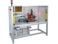
FINEPLACER® pico ama
|
|
|
| |
Features |
|
|
Benefits |
|
| |
Automated pattern recognition, alignment and bonding
Overlay vision alignment system with fixed beam splitter
Integrated Process Management (IPM)
Adaptive process library
Live process observation camera
Virtually unlimited range of advanced bonding technologies
|
|
|
Full automatic, user independent process
Outstanding placement accuracy and instant operation without adjustments
Synchronized control of all process related parameters: force, temperature, time, power, process environment, light and vision
Fast and easy process development
Immediate visual feedback reduces process development time
ROI savings - one machine for all applications
|
|
| |
Technologies |
|
|
Applications |
|
| |
Thermocompression
Thermosonic
Ultrasonic
Soldering (AuSn, C4, Indium, eutectic)
Adhesive technologies
Curing (UV, thermal)
Mechanical assembly
|
|
|
Laser diode, laser bar bonding
VCSEL, photo diode assembly
LED bonding
Micro optics assembly
MEMS packaging
Sensor packaging
3D packaging
Wafer level packaging (W2W, C2W)
Chip on glass, chip on flex
Flip chip (face down)
Precise die bonding (face up)
|
|
| |
Technical SpecificationsApplications |
|
| |
Placement accuracy*: |
5 µm @ 3 sigma |
|
| |
Field of view (min)1: |
2 mm x 1.5 mm |
|
| |
Field of view (max)1: |
14 mm x 10.5 mm |
|
| |
Component size (min): |
0.125 mm x 0.125 mm |
|
| |
Component size (max): |
40 mm x 25 mm |
|
| |
Theta fine travel: |
± 6° / 1 m° |
|
| |
Z-travel / resolution: |
10 mm / 0.8 µm |
|
| |
Y-travel / resolution: |
155 mm / 0.64 µm |
|
| |
X-travel / resolution: |
380 mm / 0.64 µm |
|
| |
Working area1: |
380 mm x 117 mm |
|
| |
Bonding force range1*: |
0.1 N - 50 N |
|
| |
Heating temp. (max)1,2*: |
400 °C |
|
| |
|
|
|


