| |
|
Highlights |
 |
|
Placement accuracy 3 µm*
Components from 0.1 mm x 0.1 mm to 150 mm x 150 mm*
Substrate sizes up to 350 mm x 350 mm*
Supports wafer sizes up to 12" *
Closed loop force control
Real time contrast optimization with LED lighting
Low maintenance, easy service access as a design priority
Fast conversion from die bonder to rework station*
|
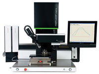
FINEPLACER® matrix ma
|
|
|
| |
Features |
|
|
Benefits |
|
| |
Automated processes
Overlay vision alignment system (VAS) with fixed beam splitter
Integrated Process Management (IPM)
Real time process observation camera
Process transfer from system to system
Virtually unlimited range of advanced bonding technologies
|
|
|
Hands-off die placement, user independent process operation
Outstanding placement accuracy and instant operation without adjustments
Synchronized control of all process related parameters: force, temperature, time, flow, power, process environment and illumination
Immediate visual feedback reduces process development time
Process transfer from R&D to production saves time, guarantees reliable results
ROI savings - one machine for all applications
|
|
| |
Technologies |
|
|
Applications |
|
| |
Thermocompression
Thermosonic
Ultrasonic
Soldering (AuSn, C4, Indium, eutectic)
Adhesive technologies
Curing (UV, thermal)
Mechanical assembly
|
|
|
Laser diode, laser bar bonding
VCSEL, photo diode assembly
LED bonding
Micro optics assembly
MEMS packaging
Sensor packaging
3D packaging
Wafer level packaging (W2W, C2W)
Chip on glass, chip on flex
Flip chip (face down)
Precise die bonding (face up)
|
|
| |
Technical SpecificationsApplications |
|
| |
Placement accuracy: |
3 µm |
|
| |
Field of view (min)1: |
1.2 mm x 0.9 mm |
|
| |
Field of view (max)1: |
15.7 mm x 11.9 mm |
|
| |
Component size (min)1: |
0.1 mm x 0.1 mm |
|
| |
Component size (max)1: |
100 mm x 100 mm |
|
| |
Theta fine travel: |
± 2° |
|
| |
Z-travel |
10 mm |
|
| |
Working area: |
310 mm x 197 mm |
|
| |
Bonding force (max)2*: |
500 N |
|
| |
Heating temperature (max)1,2*: |
400 °C |
|
| |
|
|
|


